- About basic functions and
characteristics of ICs - About scale
- About the installation
position of the scale and IC - About SMD-04 specific
questions
About basic functions and characteristics of ICs
Q
What is the basic operation of the IC?
A
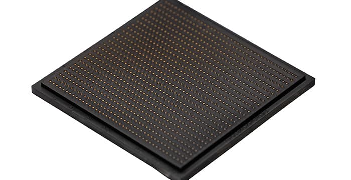
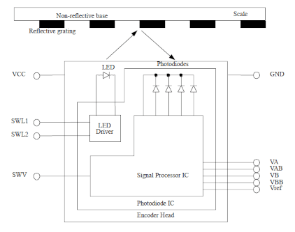
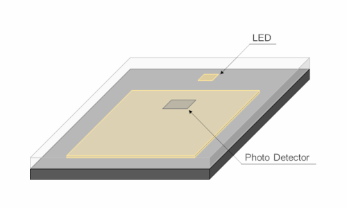
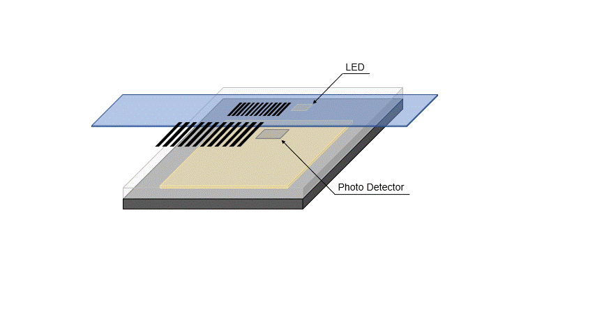
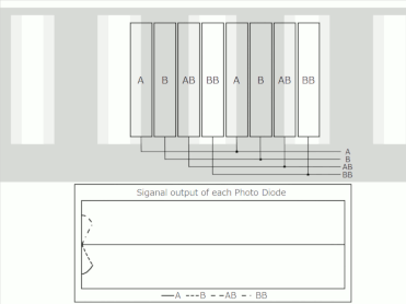
The light emitted from the LED is reflected by the scale and enters the photodetector. When the light reflected from the scale reaches the photodetector, the bright and dark patterns on the scale are designed to be magnified and projected twice as large on the photodetector surface. The scale has a 20 µm pitch pattern (10 µm reflective area and 10 µm non-reflective area), which results in a 40 µm pitch bright/dark pattern of reflected light on the photodetector. Photodetectors are arranged in the order of phase A, B, AB (inverted signal of phase A), and BB (inverted signal of phase B) at a pitch of 10 μm, so that the phase A and B signal outputs are shifted in phase by 1/4 of the pattern pitch. When the scale moves, the 40-μm pitch pattern projected on the IC also moves, so the output signal changes as the pattern moves. In this way, the movement of the scale produces a signal with a phase difference of 1/4 of a 20μm period.
Q
What is a photodetector array?
A
Photodetectors are arranged in arrays of four pairs of photodetectors for phase A, B, AB, and BB signals. The output signal is generated by averaging the outputs of multiple photodetectors for the same phase signal, making it less susceptible to partial changes in light intensity due to scale, IC surface contamination, etc. Also, if the IC is mounted on an incline, etc., the effects are canceled out because the phase A side and phase B side are affected in the same way, making it less susceptible to mounting effects.
Q
Is the 90° phase difference between phase A and B generated by internal signal processing?
A
A 20 µm pitch (10 µm light/dark pattern) scale is used to generate the phase A and B output signals by the arrangement of photodetectors in the IC. There is no function to adjust the phase difference.
Q
What is the effective wavelength range of the photodetector?
A
Photodetectors are sensitive to the entire visible spectrum (sensitivity is not constant).
Q
Is there any data on the effect of ambient light?
A
There is no specific data, but the IC contains a disturbance light cancellation circuit and is not affected by the fluorescent light in the living room.
Q
Please provide any statistical data on offset voltage and A/B phase difference.
A
There is no data that can be presented.
Q
Is it possible to use the device in a vacuum environment?
A
We have not tested the system in a vacuum, but there are some examples of it being used in a vacuum environment (vacuum level unknown).
Q
Is there any damage due to outgassing or internal rupture (collapse) under vacuum, with repeated use under normal atmospheric pressure and vacuum?
A
This has not been checked under vacuum. Unfortunately, we have no knowledge of outgassing.
Q
Please inform me of any defects that may occur if reflow soldering is carried out with the IC in a moisture-absorbing state.
A
If soldering is carried out while the body has absorbed moisture, cracks may form in the clear resin of the IC package or delamination may occur at the interface between the transparent resin and other components.
Q
I would like to reflow the back side after reflowing the IC mounting surface, is it possible to pass through the reflow proccess twice?
A
No more than one reflow process is allowed.
Q
Is there any way to use the product beyond the operating temperature range? (SMD-01)
A
Please refer to the application note. The following is an extract of the purpose. If the ambient temperature exceeds the upper storage temperature limit of 80°C for an extended period of time, the transparent resin will turn yellow. If you want to use the IC in an environment exceeding 60°C, you can use it by setting the LED brightness to low or medium, but the temperature of the IC varies greatly depending on the mounting conditions, so a careful evaluation is necessary.
Q
Is there any problem during operation and reflow (high temperature) even if there are wires etc. under the IC on the PCB/FPC board?
A
Basically, do not wire under the IC. If wiring is unavoidable, please make a decision after careful evaluation.
Q
Are SEIKO NPC encoder ICs lead-free?
A
Yes, it is lead-free.
Q
Can the package surface be cleaned with methanol?
A
If dust or dirt has been deposited, lightly moisten methanol or ethanol on soft cleaning paper with low dust emission and wipe the IC surface lightly. For other precautions, see the application note.
Q
Is there any information on the lifetime of encoder ICs?
A
Based on the long-term operation test results of SMD-01A, the lifetime is approximately 10 years under the following conditions: Ta= 60°C, LED current setting= 1x, and 8 hours of operation per day. This is not a guaranteed value, as it is the result of long-term operation tests on a single lot of ICs.
SMD-01B and SMD-04B will be tested in the future.
Q
Is it correct to understand that ripple-like waveforms appear in the waveforms of phases A and B when the servo is stopped, but disappear when the servo is switched off (de-energised), as a result of vibration?
A
Even when stopped, if the reflected light from the scale changes due to vibration, there is a possibility that a ripple-like waveform may be generated in the output signal.
Q
Is there a recommended circuit for connecting the output of an IC to the next stage IC or amplifier?
A
As the circuit and specifications of the next stage often vary greatly according to the customer's required specifications, we do not have a unified recommended circuit.
Q
I am currently receiving the differential outputs in a high impedance state, should I change this to allow some current to flow through them?
A
No. The current should be kept as low as possible, including between the differential outputs. The output current load is assumed to be around 50 uA.
Q
How much is the output impedance?
A
Based on the 30 mV/50 uA characteristic of output voltage fluctuation, the maximum is 600Ω.
Q
Please tell me how many ohms the SWV (Vref setting terminal), SWL1 and SWL2 (LED brightness setting terminals 1 and 2) terminals are internally pulled up with a resistor.
A
Terminals SWV, SWL1 and SW2 are not pulled up with resistors but with transistors. The impedance is 250k to 5MΩ (at VCC = 5V and Ta = 25°C), calculated from the values listed under input current in the specifications.
Q
How much is the output impedance?
A
Based on the 30 mV/50 uA characteristic of output voltage fluctuation, the maximum is 600Ω.
Q
If the SWV terminal is connected to GND via an external resistor, will the reference voltage change?
A
No. This terminal is a logic input and there is no purpose to change the Vref voltage with the voltage on the terminal; the voltage should match the H or L input voltage level.
Q
Is it correct to understand that if SWL1=H and SWL2=L, the signal amplitude will be 1.8Vpp?
A
The setting of SWL1=H and SWL2=L means that the current is 1.8 times larger than the current when SWL1=L and SWL2=L. There is no function to make the amplitude of the sin/cos wave to 1.8Vpp.
About scale
Q
What material is the scale made of?
A
Glass, PET, and metals are often used. Glass is often used for narrow pitch scales such as 20 µm pitch. PET and metal are used when high resolution by interpolation is not required, and PET is used when used on curved surfaces.
Q
What are the characteristics of each material of the scale?
A
Glass scales are characterised by a higher pattern accuracy and a higher reflectance of the reflective part. This means that high precision signals with large amplitudes can be obtained and high accuracy can be achieved, but in terms of thickness and size, they are at a disadvantage compared to PET and metal scales. Glass is also a hard material and cannot be used on curved surfaces. PET scales are thinner and softer than glass scales and cheaper than glass scales, but have some disadvantages such as lower pattern accuracy and narrower amplitude of output signals. Although metal scales are less precise than glass, however, metal scales are known to be more durable and resistant to corrosion than PET. As a reference, Glass scales are suitable when high accuracy and high linearity with a resolution of 1 μm or less are required by interpolation, while PET scales are suitable when the resolution is coarser than 1 µm or when the scale is mounted on a cylindrical shape, etc.
Q
I understand that PET scales are not suitable for applications with a resolution of 1µm or less, but please provide me with data to show the extent to which this is a problem.
A
PET scales are not recommended where high accuracy is required, as the structure and material of the PET scale will cause amplitude variations of up to ±10% within a given unit (±2-3% for glass scales). This is not an absolute prohibition, but should be judged in the light of the resolution required, the accuracy required and the post-processing circuit functions.
Q
What is the number of patterns on the rotary scale?
A
The scale should have a 20 µm pitch pattern at the optical centre of the IC. Therefore, the number of patterns depends on the circumference of the scale. For example, if the diameter of the optical centre is 42 mm, the number of slits is 42 mm x π/20 µm = 6597.
Q
Is it possible to obtain a test scale from your company?
A
Yes, we can supply test scales. Please contact your sales representative.
Q
Do you determine the electrical specifications using the scale introduced by the SEIKO NPC? Can you tell me how much the electrical characteristics are affected by variations in scale characteristics?
A
Standard conditions for scale, which define electrical characteristics, are listed in the specifications. Although variations in scale affect the magnitude of amplitude, there is no quantitative numerical data on the variation in scale characteristics and electrical characteristics.
Q
Is it possible to use a scale with a pitch other than 20µm?
A
Only a scale pitch of 20µm can be used; the SMD-01 and SMD-04 are designed with a scale pitch of 20µm, so the scale should be 20µm pitch (10µm reflective part/10µm non-reflective part)to match the detection period of the IC. If the scale pitch is changed, the detection period of the IC cannot be changed.
Q
I have noticed that Lissajous waveforms can be generated on ordinary metal surfaces without scale. Can a metal surface replace for a scale?
A
The phenomenon suggests that it is very likely that the metal surface happened to have a 20 µm pitch scratch across the direction of travel, which produced the output signal.
Q
Can a scale be made with 20 µm pitch unevenness by etching on a metallic material surface such as SUS304 instead of glass?
A
Even metallic surfaces can be used if the ratio of reflectivity between the reflective and non-reflective parts is large at a pitch of 20 µm (reflective part: 10 µm/non-reflective part: 10 µm) unevenness.
Q
Is the reflected light from small-diameter rotary scales fan-shaped?
A
The reflected light from the rotary scale is fan-shaped: the photodetectors of the SMD-01 and SMD-04 are arranged in a straight line, but the small size of the photodetector and the narrow scale pitch reduce the influence of different shapes. Mounting adjustments are recommended, especially when using small diameter rotary scales, as the mounting conditions are more likely to affect the amplitude and phase difference.
Q
I would like to know the effect of using a scale for SMD-04 with a Z-phase pattern on SMD-01. We are considering sharing the scale.
A
The influence of the Z-phase pattern will be 375 µm wide, including the Z-phase pattern. The effect is to reduce the incremental signal amplitude by approximately 1.5% for the SMD-01 and 1.1% for the SMD-04. There is no significant effect on the Lissajous waveform.
Q
When I use a 20µm scale for testing, which is different from the scale supplied by SEIKO NPC, the shape of the sin/cos waveform changes and an angle (edge) is produced instead of a clean circle, what is the cause?
A
Can you please inform me about the results with the glass scale supplied by SEIKO NPC? If the circle is not improved by any scale, it is considered to be an individual variation of the product.
About the installation position of the scale and IC
Q
We tested the LED light intensity setting of the SMD-01 at 2.6x, but the maximum output was only about 125 mV when the scale was moved by hand. Can this be increased when the gap with the scale etc. is best?
A
We consider that the output amplitude can be increased from the current output amplitude (125 mV) by adjusting the gap. The 0.3 mm gap value shown in the data sheet is the recommended value when using our standard glass scale; for PET scale, please make adjustments based on a gap of around 0.5 mm.
Q
Is there any way to align the optical centre point with the package outer shape as a reference point?
A
When the IC is in the same state as the 'TOP VIEW' drawing in the datasheet external dimensions, use the upper side and the left side as reference points. The tolerance of the optical centre position is ±0.2 mm when using the package outer shape as a reference point.
Q
Please let me know the Gap conditions when using the PET scale.
A
For some PET scales, the Gap amount and output amplitude characteristics were different from glass (output amplitude 0.9Vpp at Gap 0.3mm), with a peak between 0.5 and 0.6mm. Reference values at that time were: output amplitude 0.5Vpp at Gap 0.3mm, output amplitude 0.6Vpp at Gap 0.6mm.
Q
Are there any guidelines for the alignment of the encoder IC and the scale?
A
Alignment of the encoder IC and scale should be carried out with reference to the following. Gap: Position the gap between the IC and the scale where the signal amplitude is maximum and the Lissajous waveform is close to a perfect circle. (The maximum signal amplitude is around 0.3 mm for the glass scale used in the SEIKO NPC and around 0.6 mm for the PET scale.) X, Y (for rotary scales): Position where the signal amplitude is large when the scale is rotated 360° and where signal amplitude fluctuations are suppressed. Roll: If there is a large phase difference in the output signal, try adjusting the roll. Yaw, Pitch: Position where the signal amplitude is large and the Lissajous is close to a perfect circle.
Q
If a resolution of 1µm or less is required, you say that it is necessary to align the output signal during observation, please let me know what and how much affect this has on the resolution.
A
Unfortunately no data are available. It is necessary to meet the input specifications of post-processing circuits such as interpolation circuits, and although not required, it is desirable to align while observing the output signal.
Q
Please tell me the output voltage when the SMD-01 is installed in the best position. Please tell me how many volts the output signal is output.
A
The output signal amplitude when the SMD-01 is installed in the best position is the voltage in the range of 0.13 Vpp to 3.0 Vpp as stated in the specification sheet. LED light intensity also has a significant affect on the output signal amplitude, and as LED light intensity has a lot-to-lot and individual variation, we cannot specify how many volts the output voltage will be when the SMD-01 is installed in the best position.
Q
In my understanding, the best position is where the Lissajous waveform is closest to a perfect circle, but which signal should I be looking at - VA, VAB, VB or VBB?
A
To bring the Lissajous closer to a perfect circle, we recommend that you first adjust the Gap. This is because it is expected to improve the Lissajous shape compared to other installation characteristics, while minimising the affect on the signal amplitude. However, there is no quantitative data and it is not possible to judge whether the Gap to be adjusted is narrower or wider based on the specific Lissajous shape. With regard to the phase difference, it is possible to check two signals, VA (or VAB) and VB (or VBB), and not all four signals are required. If the phase difference is large, the characteristics can be improved by adjusting the roll rotation.
Q
When using a rotary scale, the application note describes that the optical centre and the centre of the scale pattern must be correctly aligned. If the diameter of the scale pattern centre is Φ40 mm, how much misalignment is allowed?
A
The affect of encoder and scale misalignment causes a deterioration in the analogue characteristics of the output waveform. The affect is dependent on the amount of misalignment and there is no sudden stopping of the function after a certain amount of misalignment. The affect on accuracy and resolution due to the degradation of analogue characteristics depends on the processing in the subsequent stages and the accuracy and resolution requirements, so it is not possible to give a general range of no affect.
Q
Please inform me of the phenomenon that occurs when the rotary scale is misaligned.
A
The following affects can be assumed by using the simplified model with regard to phenomena caused by misalignment. However, please make a full evaluation of the actual impact in the actual environment of use. [Y-direction misalignment] Y-axis misalignment is similar to roll misalignment on a linear scale. The position misalignment may cause a decrease in the amplitude of the phase A and B signals and a change in the phase difference. If the scale diameter is assumed to be Φ = 40 mm, the amount of misalignment and its affect can be assumed as follows. A misalignment of ±0.1mm will result in a 1% decrease in signal amplitude and a phase difference of approximately 0.5 to 1 degree. A misalignment of ±0.4mm will result in a 10% decrease in signal amplitude and a phase difference of 2 to 5 degrees. [X direction misalignment] Misalignment in the X direction is similar to yaw misalignment on a linear scale. The position misalignment can cause a decrease in the amplitude of the phase A and B signals. If the scale diameter is assumed to be Φ = 40 mm, the amount of misalignment and its affect can be assumed as follows. A misalignment of ±0.1mm results in a 2 to 3% reduction in signal amplitude. A misalignment of ±0.4mm results in a 10% decrease in signal amplitude.
Q
Please let me know the definition of phase difference?
A
The phase difference is calculated from the ellipse obtained by elliptic approximation of the A/B phase measurement data using the least-squares method.
Q
Why is the Lissajous waveform of the output signal distorted and what can be done about it?
A
The reason is due to dimensional variation of optical components in the IC, mounting variation of components, mounting error with the scale, etc. Since the contrast of the reflected light changes by adjusting the gap to the individual environment, use a position where the signal amplitude is large and the distortion is small.
About SMD-04 specific questions
Q
Even with APC enabled, the amplitude changes when the distance between the sensor and the scale is changed. Please let me know how APC works.
A
APC changes the LED current according to the amount of light received by the compensation PD. The purpose is to compensate for individual variations in LED light intensity, and there is no function to directly stabilize the amplitude change depending on the distance from the scale.
Q
When SWV, which can switch Verf to 1.45V or 2.25V, is set to 1.45V (SWV=H), the Z signal is always off. Please let me know if this is correct operation.
A
In this setting the Z signal output is an open drain output and should be pulled up externally.
Q
Can SMD-04 be used with scale without pattern for Z-phase?
A
It can be used, but SEIKO NPC has only checked that it can be used with Kosib's glass scale.
Q
There is a chatter on the Z-phase signal, is there any way to adjust the mounting to improve it?
A
It may be improved by adjusting X, Y, Roll, and Pitch. When using a rotary scale, adjust X and Y to a position where the amplitude of the incremental signal fluctuates little when the scale is rotated 360°. If there is misalignment, the incremental signal will fluctuate like an amplitude-modulated signal.
Q
The Z signal has rough edges and cannot be used. The pulses are not clean, but there is a jittery signal at the beginning and end of the pulses. Please provide a scale that does not cause this phenomenon.
A
The SMD-04 is not equipped with a function to completely prevent the occurrence of such signals. If waveform noise is a problem, it is not necessary to change the scale, but rather to process it in the post-processing circuit to avoid affecting the system operation.
Q
What is the cause of chatter in the Z-phase signal?
A
The Z-phase signal generation circuit of the SMD-04 includes a circuit that suppresses chatter when generating Z-phase digital signals from Z-phase analogue signals, but it is not a circuit that completely prevents chatter.
Q
I would like to know the possible causes of chattering of the Z-phase signal.
A
Possible factors include the affected installation condition, dirty scale, etc.