- Basic functions and
operation of ICs - About scales and
installation of scales and ICs - About Incremental
signals - About absolute data
Basic functions and operation of ICs
Q
Please let me know the basic operation of the IC.
A
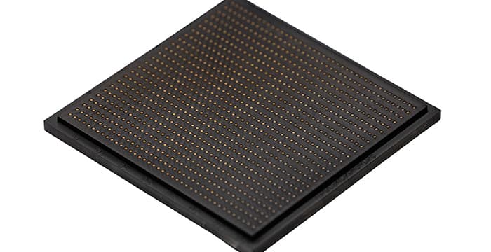
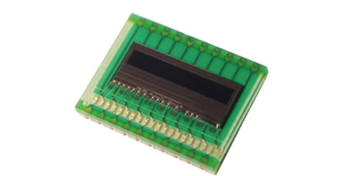
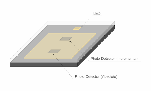
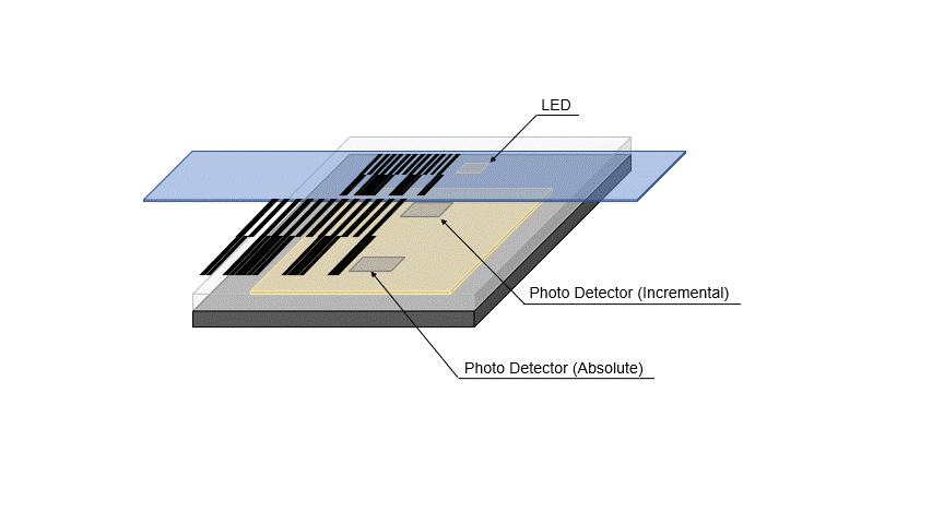
The IC package contains an LED for light emission and an IC for photodetector. The light emitted from the LED is reflected by the scale and enters the photodetector. By arranging the scale and IC as described in the datasheet, the light and dark patterns reflected by the incremental and absolute patterns on the scale are designed to be magnified and projected twice as large on each photodetector surface. The scale has a 100μm pitch pattern for incremental use (50μm reflective area and 50μm non-reflective area) and a pattern for absolute where one bit is recorded as a reflective or non-reflective area with a width of 100 μm, and on the photodetector reflected light becomes a bright/dark pattern with a 200μm pitch, and one bit becomes a 200μm bright/dark pattern. Two types of photodetector arrays are available on the IC: a photodetector array with multiple photodetectors for incremental signals and a photodetector array for absolute signals. Photodetectors for incremental signals are arranged in the order of phase A, phase B, phase AB (inverted signal of phase A), and phase BB (inverted signal of phase B) at a pitch of 50μm. When the scale moves, the 200μm pitch pattern projected on the IC also moves, so the output signal changes as the pattern moves, and the 100μm pitch scale (pattern on the scale) moves, resulting in the output of a signal with a phase difference of 1/4 of a period of 100μm. There are 20 photodetectors for absolute signals, including 9 even-numbered photodetectors and 9 odd-numbered photodetectors arranged alternately at a 100μm pitch, plus one dummy at each end. The 9bit absolute data is generated from the outputs of the even-numbered 9 photodetectors and the odd-numbered 9 photodetectors. When the scale is moved, signals for 1 bit of the absolute pattern are output from the odd-numbered photodetectors and the even-numbered photodetectors at positions 100μm shifted.
Q
What is a photodetector array for incremental signals?
A
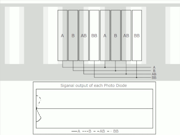
Photodetectors are arranged in arrays of four pairs of photodetectors for phase A, B, AB, and BB signals. The output signal is generated by averaging the outputs of multiple photodetectors for the same phase signal, making it less susceptible to partial changes in light intensity due to scale, IC surface contamination, etc. Also, if the IC is mounted on an incline, etc., the effects are canceled out because the phase A side and phase B side are affected in the same way, making it less susceptible to mounting effects.
Q
Is the 90° phase difference between phase A and B generated by internal signal processing?
A
A 100µm pitch (50µm bright/dark pattern) scale is used to generate the phase A and B output signals by the arrangement of photodetectors in the IC. There is no function to adjust the phase difference.
Q
What is the effective wavelength range of the photodetector?
A
Photodetectors are sensitive in the visible to near-infrared wavelength range (sensitivity is not constant).
Q
Is there any data on the effect of ambient light?
A
There is no specific data, but the SM3414 may be affected by strong light entering the SM3414.
Q
Could you please give me some information on the spectral distribution of LEDs.
A
850nm is the peak of the intensity distribution and there is more than 5% of the peak intensity in the range of about 800nm to 870nm.
Q
Can the package surface be cleaned with methanol?
A
If dust or dirt has been deposited, lightly moisten methanol or ethanol on soft cleaning paper with low dust emission and wipe the IC surface lightly. For other precautions, see the application note.
Q
Even if the mounting tolerance is smaller than the specification, is it necessary to set and read out the various registers individually?
A
Because of the affect of not only mounting but also element variation, it is necessary to set the appropriate registers and select the correct ABS code.
Q
I am considering using VDD and LED_VDD on the same power supply, but is there anything I should be aware of?
A
It is possible to connect VDD and LED_VDD and use them on the same power supply, but depending on the LED current, LED_VDD may require a higher voltage than VDD. In such cases, if LED_VDD is lower than the required voltage, the LED current will saturate and the required current will not flow.
Q
Does LED current adjustment always require real-time current adjustment?
A
There is no need to adjust the LED current in real time; the purpose is to correct the light emission due to individual LED differences. When the IC is not in use, the LED current can also be turned off by powering down the LED_CON input voltage.
About scales and installation of scales and ICs
Q
What is the M code?
A
M codes are binary codes encoded in the M-sequence, and the SM3414 uses codes encoded using a linear feedback shift register. The feature of this code is that n bits of data can represent n powers of 2 total data, and between a one data and the data before or after it, the (n-1)-bit data is shifted by 1 bit with the value as it is, and the most significant or least significant bit is the value obtained by exclusive or of the original n bits of data. This feature can be applied directly to absolute patterns, and in the SM3414, when the scale moves by 1 bit, the 8-bit pattern is shifted by 1 bit and a new 1-bit pattern is used. As a result, it is possible to locate 512 positions in a single track pattern.
Q
The SM3414 scale has two patterns, incremental and absolute. Are there any precautions regarding the mounting position of the IC and scale that are different from those of the incremental encoder?
A
As described in the data sheet, the incremental and absolute patterns are projected at an angle to the photodetector when there is a yaw misalignment. As a result, there will be a phase difference between the incremental and absolute signals, and it may be necessary to change any method of selecting the absolute information to be read according to the level of the incremental signal.
Q
Is it possible to obtain a test scale from your company?
A
Yes, we can supply test scales. Please contact your sales representative.
About Incremental signals
Q
Is it ok to connect VDD and LED_VDD at the same time to start the power supply?
A
There is no problem to connect VDD and LED_VDD and power them up at the same time.
Q
The maximum output frequency of incremental signals is 10 kHz. What happens if the frequency is exceeded?
A
There is a possibility of a decrease in output amplitude and worsening distortion of the sinusoidal output waveform.
Q
The incremental signal output signal amplitude ranges from 0.18 to 0.70 Vpp. Is this due to individual variability?
A
The specification of incremental signal output signal amplitude is dominated by individual variation.
Q
Are there any specifications regarding the output amplitude variations between PA and PB signals for incremental signals?
A
There is no guaranteed value in the specifications for PA and PB signals of the same unit, but it should be expected to be in the tens of mV range.
The main factors are individual LED variation and IV conversion resistor variation.
Q
What is the accuracy of the offset voltage (0.5VDD) of the incremental signal?
A
There is no specification for the offset, but there is a variation of several tens of mV.
Q
Am I correct in understanding that the incremental signal has an output voltage amplitude of 0.18-0.35-0.7 Vp-p under the conditions described in the data sheet (e.g., 0 dB gain setting), and that the output can be adjusted to saturation by setting the GA/GB gain?
A
This is correct, but if the gain setting is too high or the LED current is too much, the incremental output will saturate around 0[V] or VDD[V].
Q
Do you have data on individual variations in output amplitude?
A
Unfortunately, there is no data that we can provide.
Q
Please provide any statistical data on offset voltage and A/B phase difference.
A
Unfortunately, there is no data that we can provide.
About absolute data
Q
Please let me know the guideline for setting the absolute binarization threshold voltage adjustment function and an example of the setting.
A
The setting value depends on the amplitude of the incremental and absolute signals. Set the target around 40% to 50% of the amplitude of the absolute signal. Refer to the data sheet and application note for details.
Q
Is "ABS code 1 or 2" automatically selected inside the SM3414?
A
The customer must select and read from the internal register. ABS_DATA (odd number) corresponds to ABS code 1 and ABS_DATA (even number) corresponds to ABS code 2.
Q
What is the purpose of selecting even PD and odd PD in the ABS_DATA register?
A
At the timing when the level of the absolute signal changes, the binarized internal absolute code (ABS CO) also changes, and if data is read out at this timing, the conversion from M code to binary code will not be performed correctly. By setting the appropriate VCOMP voltage, the switching timing can be made wider, and the data on the stable side can be read out with even and odd PDs depending on the incremental signal level.
Q
Please let me know the specific procedure for changing the readout of absolute data according to the level of incremental signals.
A
Please perform the readout in the following order.
(1) Detect the phase of the incremental signal by the voltage of PA or PB.
(2) Decide the even/odd selection (SEL[2:0]) from the detected phase and send a read command.
(3) The SM3414 internally determines the serial output data by converting the selected binary absolute signal (M code) to binary code at the timing when the addressing A[2:0] following SEL[2:0] is input.
(4) Reads the data output from the SM3414 after addressing A[2:0] as absolute data.